EVAL-AD7490-ARDZ
Arduino Compatible Evaluation Board for AD7490
Overview
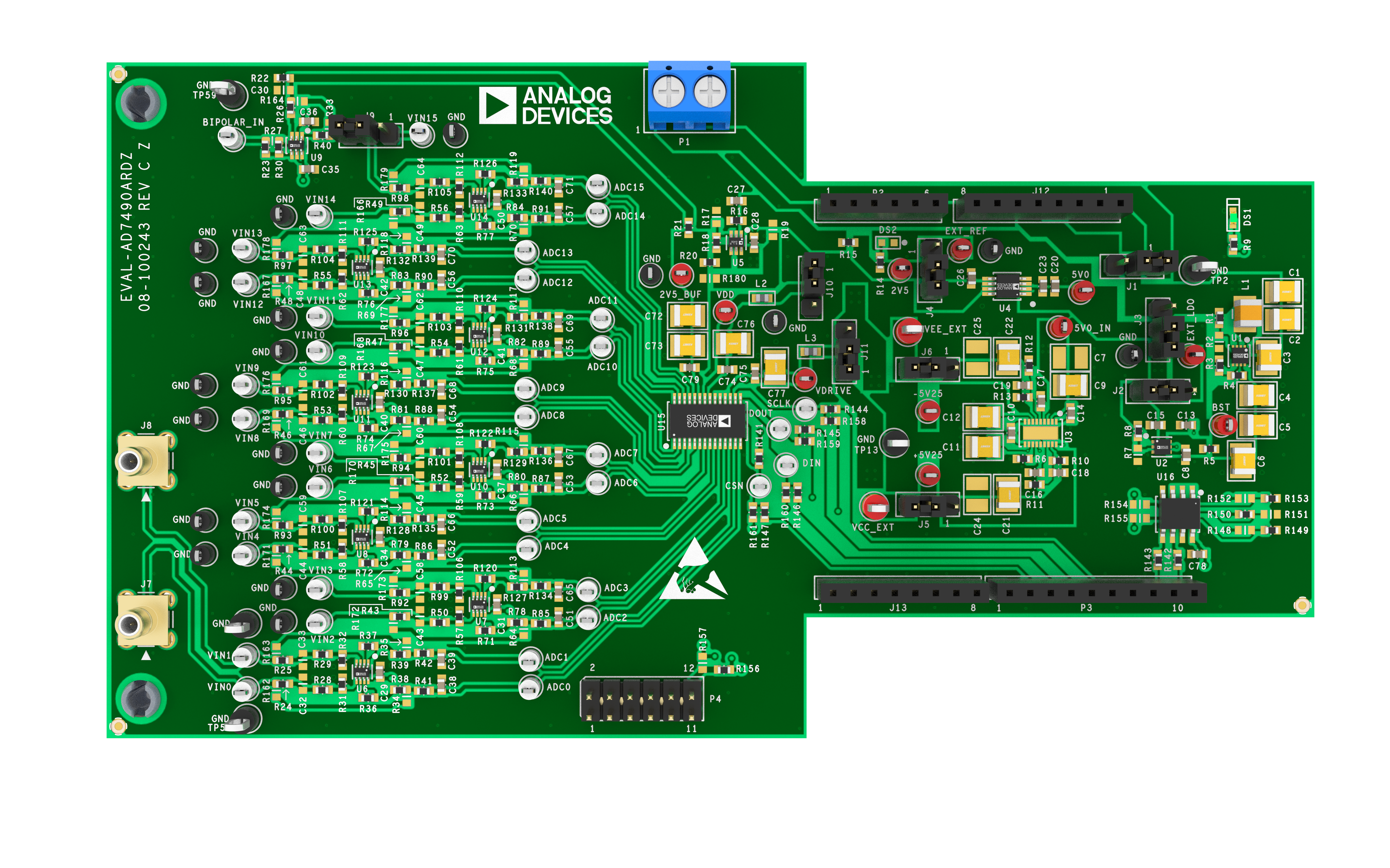
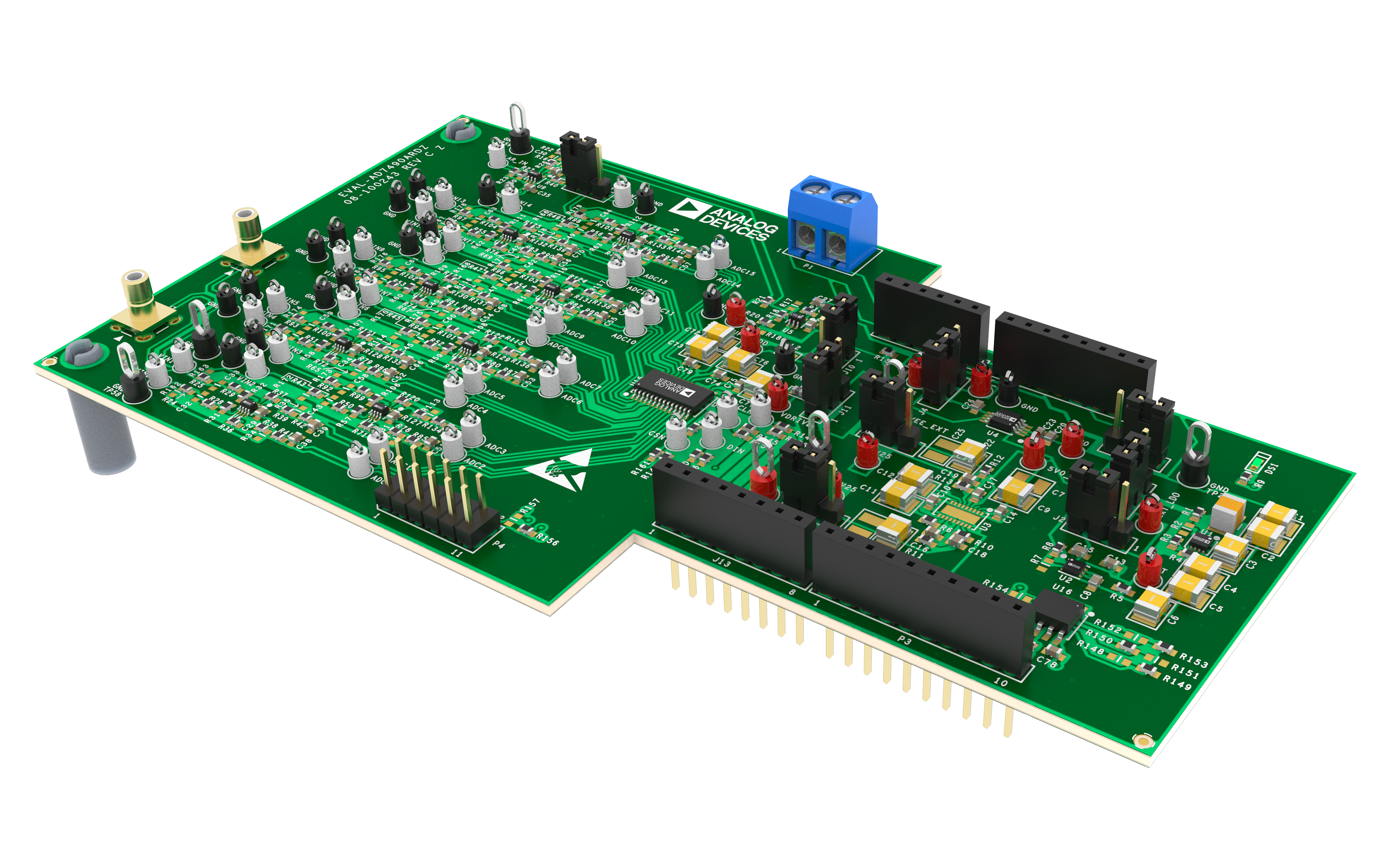
The EVAL-AD7490-ARDZ is an Arduino compatible evaluation board for evaluating all features of AD7490. The AD7490 is a 12-bit, 16-channel, high speed, low power, successive approximation (SAR) ADC that operates from a single 2.7 V to 5.25 V power supply and features throughput rates of up to 1 MSPS. The evaluation board can be controlled via the SDP-K1 (EVAL-SDP-CK1Z) board which enables control and data capture via the PC’s USB port. The EVAL-AD7490-ARDZ can be powered directly from USB via the SDP-K1 controller board, or via an external 5 V supply. To facilitate the low noise voltage supply requirements and standalone operation, the EVAL-AD7490-ARDZ features the following components on board:
MAX17291: Low I:sub:Q Current DC-DC Boost Converter
ADP7118: 200mA Low Noise CMOS LDO
ADR3625: Precision Micropower Voltage Reference
MAX44260: 1-channel 15MHz Low-Offset Low-Power Rail-to-Rail Op-Amp
MAX44263: 2-channel 15MHz Low-Offset Low-Power Rail-to-Rail Op-Amp
ADA4807-1: 1-channel 180 MHz Low Noise Rail-to-Rail Op-Amp
LTC3265: Low Noise Dual Supply with Boost and Inverting Charge Pumps (provision only)
|
|
Features
Fully featured evaluation board for AD7490
PC-based control when used with the SDP-K1 controller board (EVAL-SDP-CK1Z)
Arduino UNO–compatible form factor and pin configuration
Supports standalone operation
Accepts 0 V to 5 V unipolar input signals on all ADC channels
Supports −2.5 V to +2.5 V bipolar input on VIN15 channel
Supports input signal frequencies from 0 to 500kHz
Includes drivers for embedded firmware and software development
Compatible with ACE software plugin for control and data analysis (time and frequency domains)
Applications
Multichannel system monitoring
Battery-powered equipment
Power line monitoring
Data acquisition, instrumentation, and process control
Package Contents
EVAL-AD7490-ARDZ Evaluation Board
Additional Equipment Needed
EVAL-SDP-CK1Z controller board (must be ordered separately and includes a USB-A to USB-C cable)
Signal generator
PC running Windows 10/11 with ACE software installed
External DC power supplies
Block Diagram
Hardware Description
The EVAL-AD7490-ARDZ is an Arduino form factor evaluation board for AD7490 featuring essential on-board circuitry to support both full feature and standalone operation. It can accept unipolar input signals between 0 V to 5 V on all channels (VIN0 to VIN15) and can also be configured to accept bipolar input signals between -2.5 V to +2.5 V on channel VIN15. For more information on AD7490, please refer to the device datasheet.
Power Supply Section
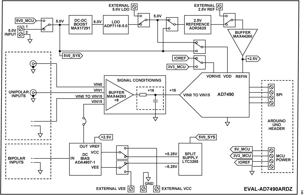
The board can be powered either by an external 5 V DC source or through the SDP-K1 controller via the Arduino header. The 5 V input is boosted to ~6 V using the MAX17291 and then regulated by the ADP7118-5.0 LDO to provide a stable on-board 5 V rail. This regulated supply powers critical components, including the AD7490 VDD, analog front-end circuitry, DC bias generator, and ADC reference.
An optional LTC3265 charge pump (not populated by default) can generate ±5.25 V supplies for bipolar input signals on VIN15. These rails may alternatively be provided externally via test points. The ±5.25 V supply enables level shifting of bipolar inputs to a 0–5 V range.
The AD7490 VDRIVE pin powers the SPI interface and can be sourced from the SDP-K1’s 3.3 V or IOREF rail. The board also supports configuration via jumpers and test points to allow external supplies to bypass the on-board 5 V regulator and 2.5 V reference. Refer to Tables 2 and 3 for details.
ADC Reference Voltage
The on-board 2.5 V reference is generated by the ADR3625 and buffered by the MAX44260 to drive the AD7490 REFIN pin and the DC bias circuit. This rail can be bypassed to accept an external low-noise 2.5 V source. Refer to Tables 2 and 3 for configuration details.
Analog Front-End (AFE) Circuitry
The analog front end comprises eight dual-channel MAX44263 buffers and sixteen identical RC low-pass filters that condition inputs prior to the AD7490. All channels support 0–5 V unipolar signals, with filter cutoff set to ~505 kHz. Refer to Table 2 for ADC channel input test points.
DC Bias Generator
The DC bias generator uses an ADA4807-1 configured as a difference amplifier to shift bipolar inputs to a unipolar range for the AD7490 VIN15 channel, producing an inverted AC component. It requires ±5.25 V rails supplied externally or via the optional LTC3265. This function is available only on VIN15. Refer to Tables 2 and 3 for configuration details.
SPI Interface
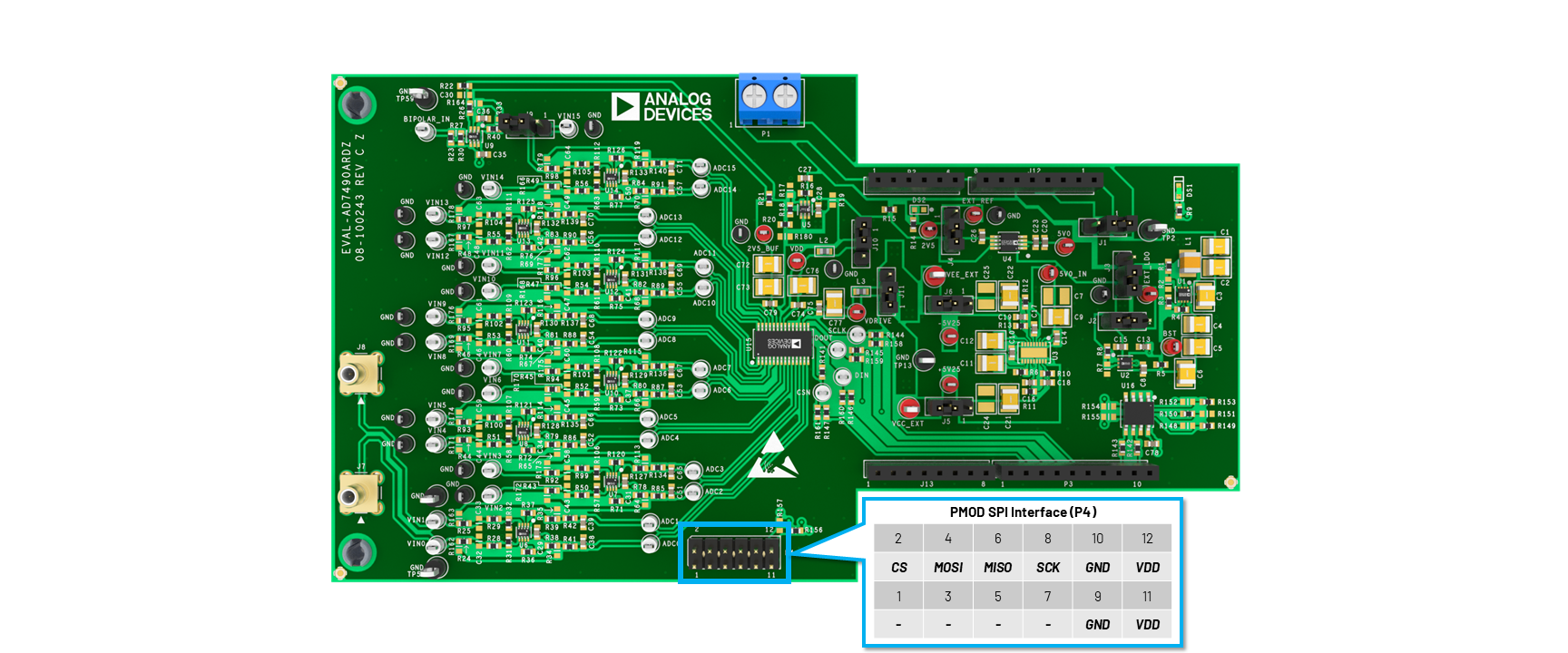
The AD7490 supports multi-channel data acquisition via its SPI interface, with signals routed to the Arduino header using standard pin assignments. An on-board 12-pin PMOD connector provides access to the same SPI lines for flexible controller interfacing. Refer to the image and Table 1 below for pin details.
Test Points and Jumper Locations
Table 2 and table 3 summarizes the test points and jumper locations on the board with detailed description for each.
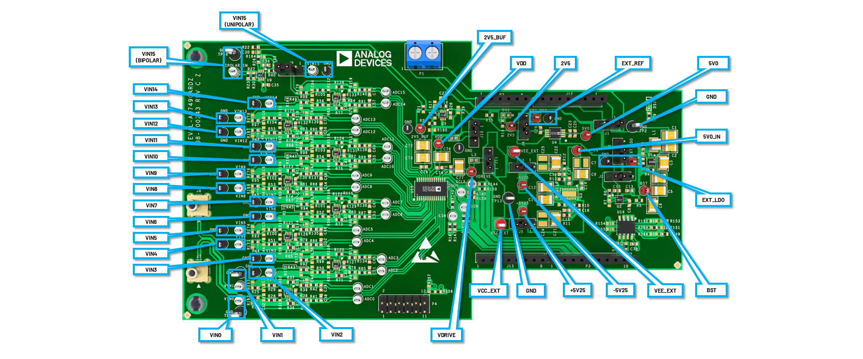
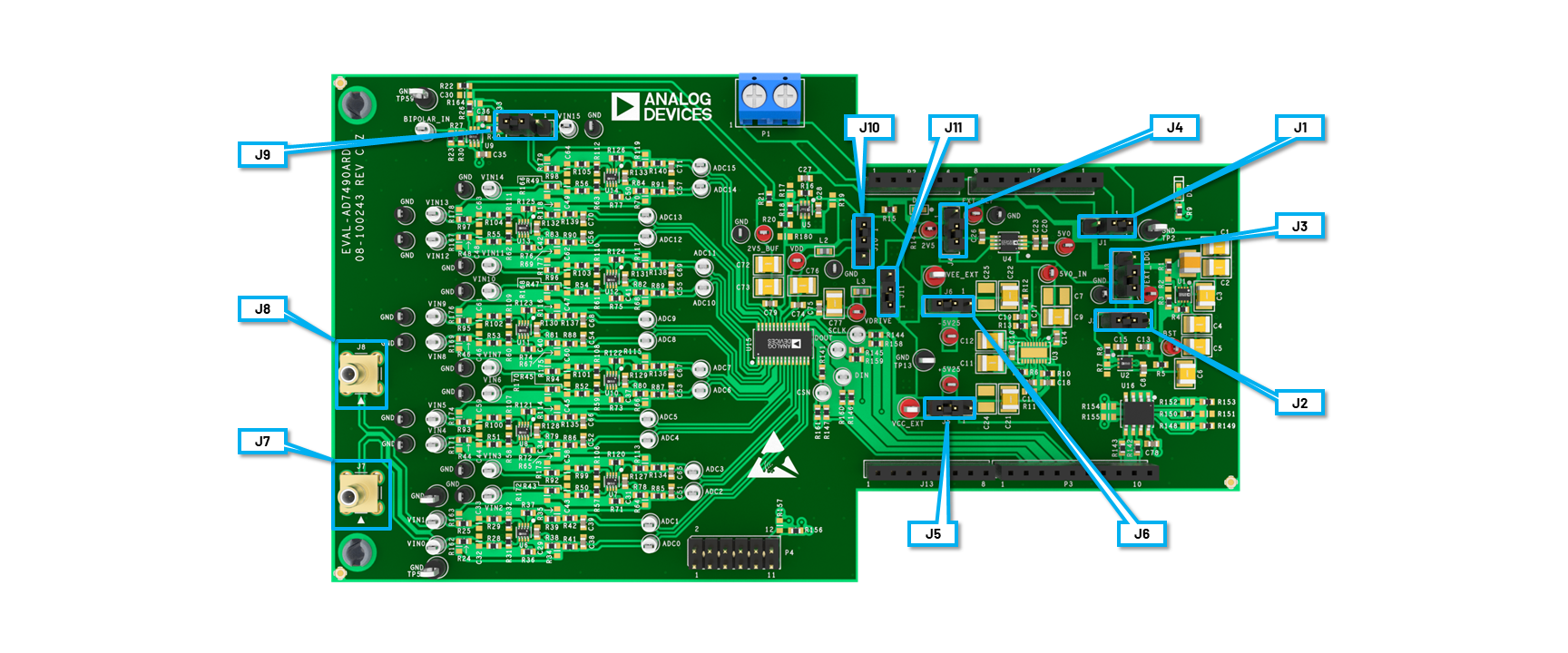
Board Specifications
Parameter |
Minimum |
Typical |
Maximum |
Unit |
Remarks |
|---|---|---|---|---|---|
External Input Supply |
1.8 |
5.0 |
5.5 |
V |
Connects to P1 |
Bipolar Input Voltage Range |
-2.5 |
- |
+2.5 |
V |
VIN15 only |
Unipolar Input Voltage Range |
0 |
- |
5.0 |
V |
All ADC input channels (VIN0 - VIN15) |
Input Signal Frequency |
- |
- |
500 |
kHz |
All ADC input channels (VIN0 - VIN15) |
ADC Sampling Rate |
- |
1 |
- |
Msps |
- |
SNR |
65 |
- |
- |
dB |
50kHz sine wave input, -0.5 dBFS fundamental power, 950kHz sampling rate |
THD |
- |
- |
-65 |
dB |
50kHz sine wave input, -0.5 dBFS fundamental power, 950kHz sampling rate |
SINAD |
64 |
- |
- |
dB |
50kHz sine wave input, -0.5 dBFS fundamental power, 950kHz sampling rate |
ENOB |
10.2 |
- |
- |
bits |
50kHz sine wave input, -0.5 dBFS fundamental power, 950kHz sampling rate |
SFDR |
68 |
- |
- |
dB |
50kHz sine wave input, -0.5 dBFS fundamental power, 950kHz sampling rate |
Hardware Setup
The evaluation board caters to a combination of setup configurations depending on the user application. These are determined by the input supply options and the type of input signals (unipolar or bipolar) being evaluated.
Evaluating Unipolar Test Signals
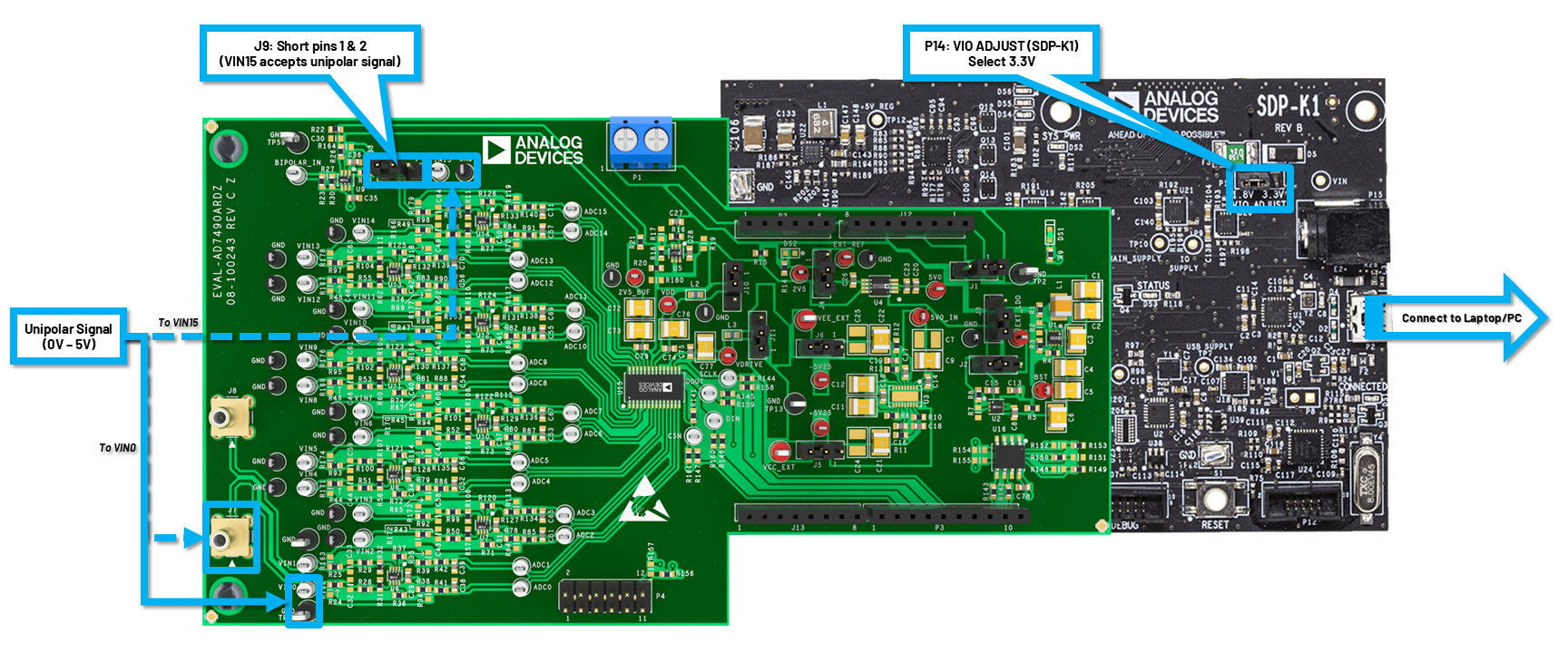
By default, the EVAL-AD7490-ARDZ accepts unipolar signals on VIN0–VIN14. To enable unipolar input on VIN15, short pins 1 and 2 of J9, then connect the input signal to the designated test point as shown below:
Evaluating Bipolar Test Signals
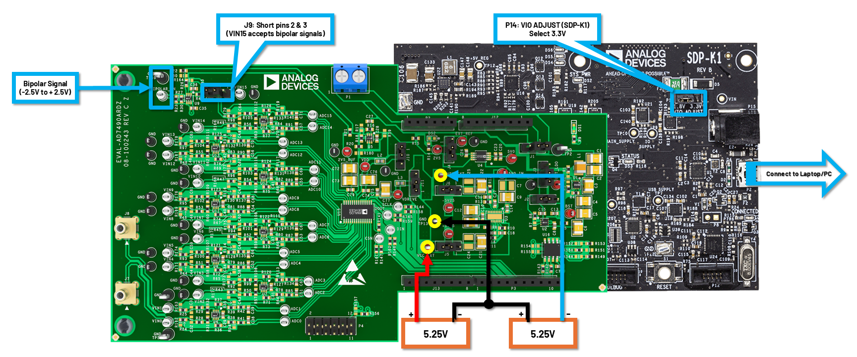
Bipolar signals are supported only on VIN15. To enable this, short pins 2 and 3 of J9 and connect the input to the VIN15 (Bipolar) test point (see Figure 4). A 2-channel isolated DC supply configured for ±5.25 V is required: connect the midpoint to GND, +5.25 V to VCC, and −5.25 V to VEE, as shown below.
Using External 5.0 V Supply
An external 5.0V supply can be used to power the board separate from the controller. This can be configured by connecting the external 5.0V supply to P1 and shorting pins 1 & 2 of J1 as shown below:
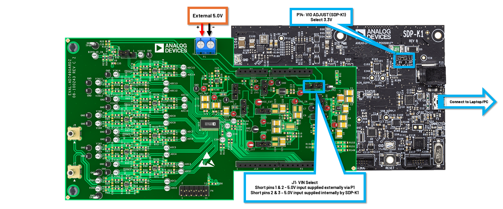
Example Setup - Evaluating Bipolar and Unipolar Signals
This section describes the hardware setup for evaluating both unipolar and bipolar types of signals without using an external 5.0V supply. This enables evaluation of unipolar signals on VIN0-VIN14 and assigning VIN15 as the dedicated input for bipolar signals. This setup requires the following equipment and/or materials:
1x EVAL-SDP-CK1Z (SDP-K1 controller board)
1x Signal Generator
1x 2-channel isolated DC power supply
PC/Laptop running Windows 10/11
1x BNC to Test Clip cable
1x USB (type-A to type-C or type-C to type-C) power and data cable
Banana Jacks, Plugs, and extra Test Clip cables
Setup Procedure
Configure the EVAL-AD7490-ARDZ board to use the 5.0 V supply provided by the Arduino header by shorting pins 2 and 3 of J1.
Configure the EVAL-AD7490-ARDZ board to accept bipolar signals on VIN15 by shorting pins 2 and 3 of J9.
Locate the P14 (VIO_ADJUST) jumper on the SDP-K1 controller board and set it to 3.3 V.
Mount the EVAL-AD7490-ARDZ board to the SDP-K1 controller board.
Set the output voltage of each channel of the 2-channel isolated DC supply to 5.25 V, and the OCP limit to at least 100 mA. Do not turn on the channels of the power supply at this point.
Connect the 2 channels of the isolated DC supply in series. Connect their midpoint to GND, +5.25 V to VCC, and −5.25 V to VEE test point of the EVAL-AD7490-ARDZ board.
Connect the USB-C port of the SDP-K1 controller board to the PC via USB cable. The two LEDs (DS1 and DS2) on the eval board should light up shortly after.
Turn on the two channels of the isolated DC supply to enable the DC bias circuitry on VIN15.
Configure the output of the signal generator to generate ADC test signals from 0 up to 500kHz:
Unipolar test signals - Connect the output of the signal generator to any channel from VIN0 - VIN14. Make sure that the signal level does not exceed the specified range of 0 - 5 V.
Bipolar test signals - Connect the output of the signal generator to VIN15. Make sure that the signal level does not exceed the specified range of -2.5 V to +2.5 V.
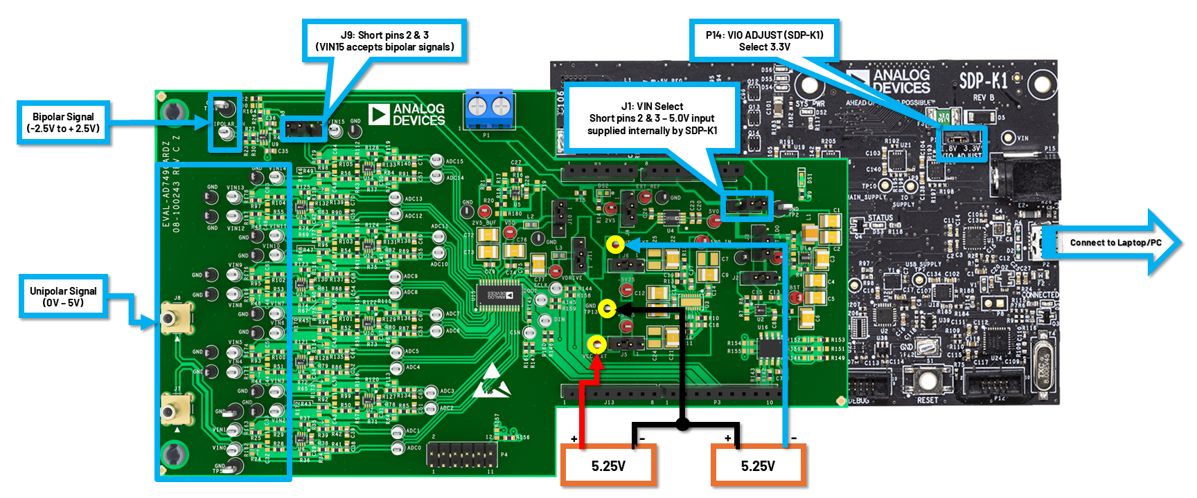
Figure 10 Setup for Evaluating Unipolar and Bipolar Signals, Internal 5.0 V Supply
Once configured, proceed to the Software Setup section to download and install the complementary evaluation software for EVAL-AD7490-ARDZ using ACE.
Software Setup
The EVAL-AD7490-ARDZ is supported by ADI’s Analysis | Control | Evaluation (ACE) software for control, data capture, and data analysis. This section provides the step-by-step procedure for the required prerequisites prior to evaluation using ACE.
Installing ACE Software
Download and install ADI’s ACE software through this link: Analysis | Control | Evaluation (ACE).
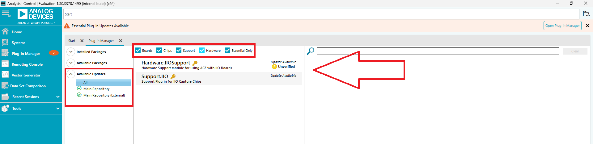
After installation, check if the Plug-in Manager prompts for any essential updates.
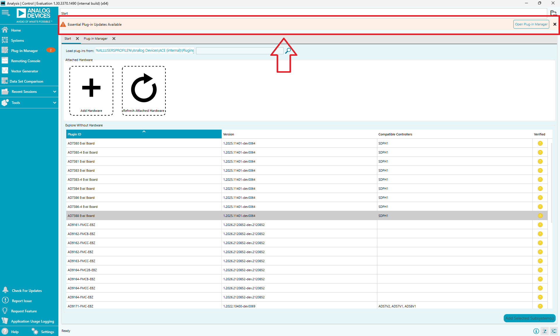
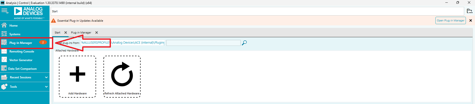
Click on the Plug-in Manager tab on the left panel to update essential plug-ins.
Click on Available Updates, and check all plug-in types (Boards, Chips, Support, Hardware, Essential Only). This will display all essential plug-in types that need to be updated.
Once all essential plug-ins are listed, click the Update All button at the bottom, wait for the update process to finish and then, restart ACE.
Installing ACE Plugin Support for EVAL-AD7490-ARDZ
In order for ACE to properly detect and capture data from the hardware setup, the board plug-in for AD7490 should be installed in ACE. To install:
Click on the Plug-in Manager on the left panel.
Click on Available Packages and then, click on the Boards and Chips checkbox.
Type “AD7490” on the search entry. The corresponding plug-ins for AD7490 should appear as listed similar to the image below:

Select both plugins by clicking on each entry while holding the CTRL key.
Click on the Install Selected button at the bottom and then, Restart ACE.
Uploading the tinyIIOd firmware to SDP-K1
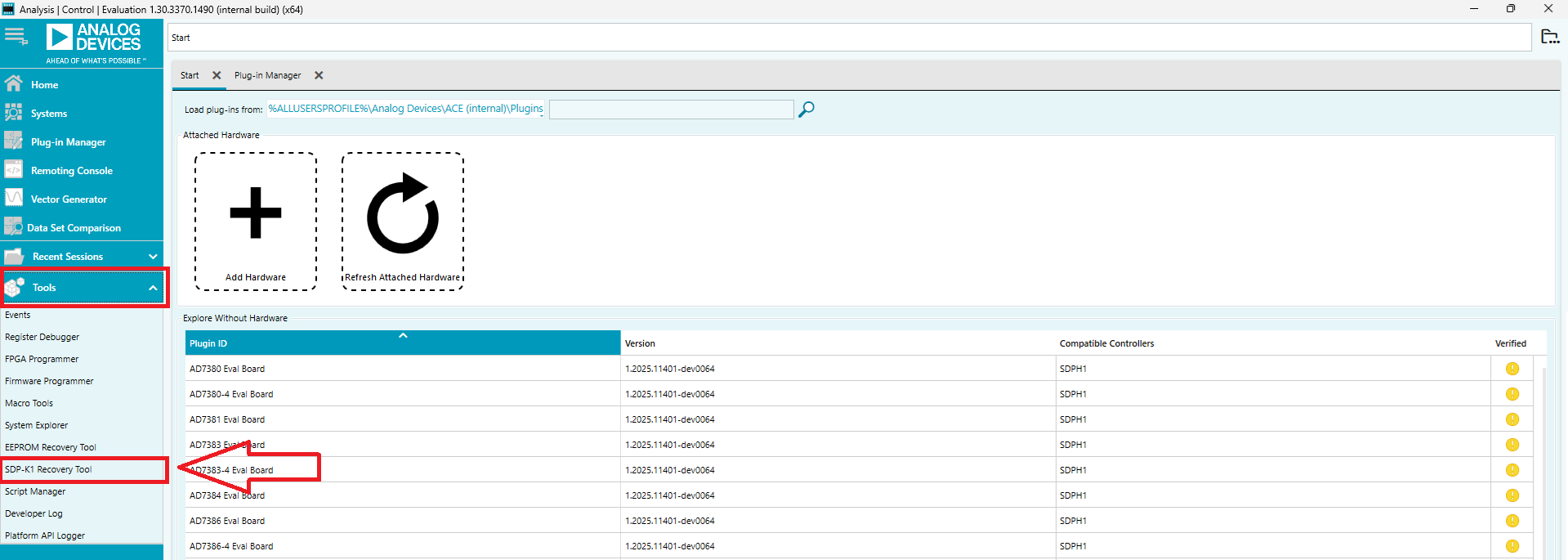
Given that the SDP-K1 controller board is sourced separately, it does not come preloaded with the tinyIIOd firmware that can communicate to the ACE software and plug-ins. To install the appropriate firmware, ACE’s internal SDP-K1 Recovery Tool will be utilized.
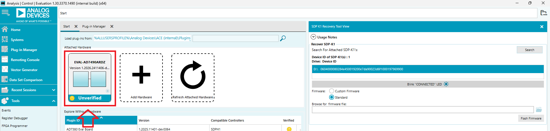
Launch the ACE software and under the Tools tab on the left panel, click on the SDP-K1 Recovery Tool.
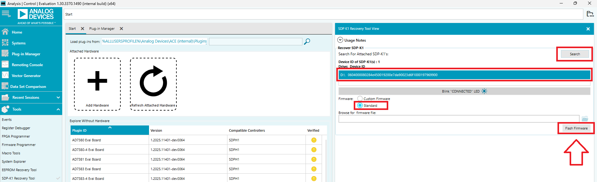
The SDP-K1 Recovery Tool view should pop-up from the right panel. Click on the Search button to detect the SDP-K1 board attached to the PC.
Click on the device ID of the detected SDP-K1 board and click on the Standard Firmware option.
Lastly, click the Flash Firmware button and wait for the firmware upload to finish.
Note
After successful upload of the default firmware, ACE will be able to automatically detect the mounted evaluation board, and a pop-up should appear prompting to upload the dedicated evaluation firmware.
Click the OK button on the pop-up window and wait for the firmware upload to finish.
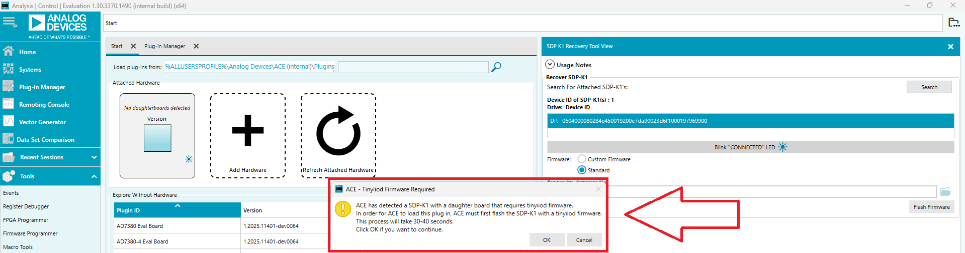
Once the evaluation firmware has been uploaded, ACE should now be able to detect the evaluation board and display the correct hardware name in the Attached Hardware panel.
Note
After successful completion of the previous steps, the setup is now ready for evaluation using ACE.
Once ACE has detected the hardware setup, double click on the plugin icon in the Attached Hardware panel to open the board view and refer to the built-in plugin documentation for AD7490 for details on evaluating ADC test signals using the EVAL-AD7490-ARDZ evaluation board.
Software Resources
AD7490 PyADI-IIO Example Code (PyADI-IIO library support for Python development)
ACE plug-in support for EVAL-AD7490-ARDZ via Analysis | Control | Evaluation (ACE)
Additional Resources
Design and Integration Files
Help & Support
For questions and more information, please visit the EngineerZone Support Community or contact your local ADI representative.